
A guide to the ZX Evolution Rev. C ZX Spectrum-compatible computer: board layout, connectors, firmware and installation in an ATX or mini-ITX case.
Contents
1. Board layout
The diagram shows the main components and connectors on the ZX Evolution Rev. C board.
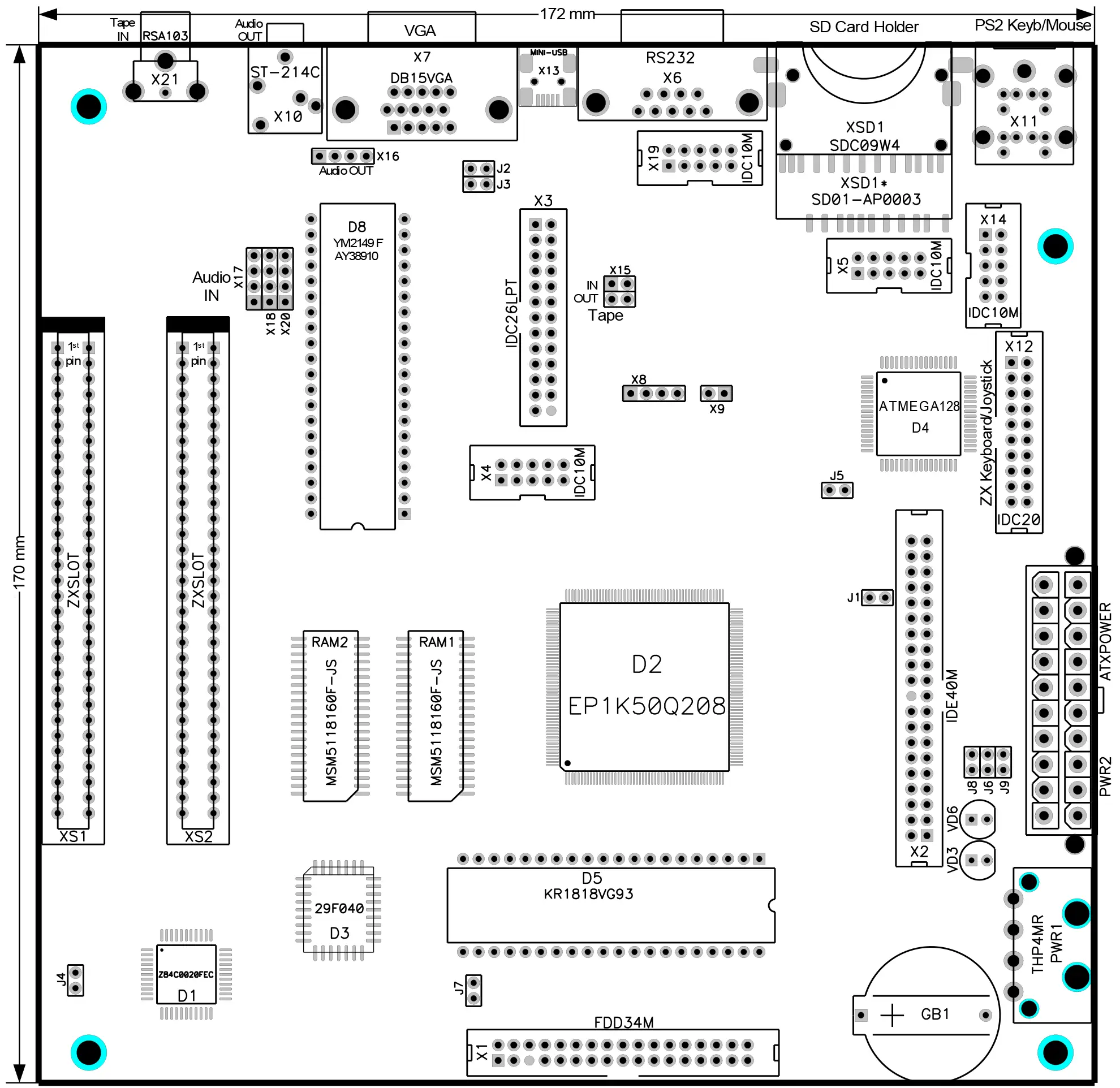
The board has mounting holes for installation in a mini-ITX case, in accordance with the specification1. The main peripheral connectors are positioned in the rear I/O opening of an ATX case, making the board easier to install and the connectors easier to access.
The expansion slots are positioned so that the connectors on installed cards line up with the corresponding openings at the back of the case. The original manual identifies NeoGS as a supported expansion card. Third-party expansion-card designers should follow the NeoGS board form factor.
A standard ATX power connector allows the board to use an off-the-shelf power supply.
1 The board measures 172 × 170 mm and is 2 mm wider than specified by the mini-ITX standard. This extra width provides the required space for the ZXBUS slot.
2. Connectors
2.1. X1. Floppy drives
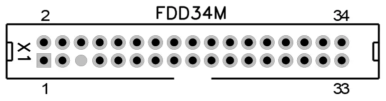
This connector accepts 3.5-inch or 5.25-inch floppy drives. Up to four drives are supported. Pin numbering starts at the square pad.
| № | Name | Description | № | Name | Description |
|---|---|---|---|---|---|
| 1 | GND | Ground | 2 | Not used | |
| 3 | GND | Ground | 4 | Not used | |
| 5 | KEY | Key (no pin) | 6 | DS3 | Drive 3 select |
| 7 | GND | Ground | 8 | IDX | Index pulse |
| 9 | GND | Ground | 10 | DS0 | Drive 0 select |
| 11 | GND | Ground | 12 | DS1 | Drive 1 select |
| 13 | GND | Ground | 14 | DS2 | Drive 2 select |
| 15 | GND | Ground | 16 | MOTON | Motor on |
| 17 | GND | Ground | 18 | DIRC | Step direction |
| 19 | GND | Ground | 20 | STEP | Step head to the next track |
| 21 | GND | Ground | 22 | WD | Write data |
| 23 | GND | Ground | 24 | WG | Write enable |
| 25 | GND | Ground | 26 | TR00 | Head at track 00 |
| 27 | GND | Ground | 28 | WP | Disk write-protect status |
| 29 | GND | Ground | 30 | RDDATA | Read data |
| 31 | GND | Ground | 32 | SIDE1 | Disk side select |
| 33 | GND | Ground | 34 | Not used |
2.2. X2. IDE
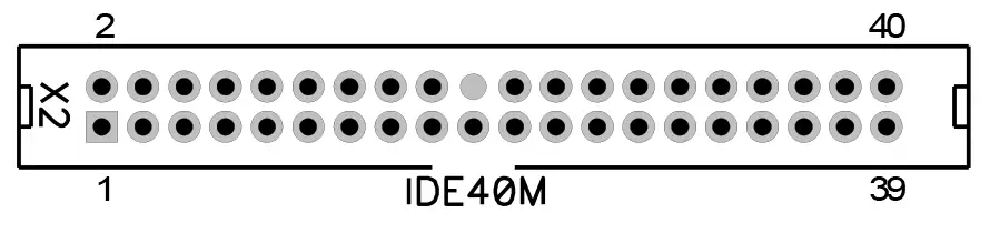
This connector accepts IDE storage devices. Up to two devices can be connected in a master/slave configuration. Pin numbering starts at the square pad.
| № | Name | Description | № | Name | Description |
|---|---|---|---|---|---|
| 1 | RESET | Hardware reset | 2 | GND | Ground |
| 3 | D07 | Data bus bit 7 | 4 | D08 | Data bus bit 8 |
| 5 | D06 | Data bus bit 6 | 6 | D09 | Data bus bit 9 |
| 7 | D05 | Data bus bit 5 | 8 | D10 | Data bus bit 10 |
| 9 | D04 | Data bus bit 4 | 10 | D11 | Data bus bit 11 |
| 11 | D03 | Data bus bit 3 | 12 | D12 | Data bus bit 12 |
| 13 | D02 | Data bus bit 2 | 14 | D13 | Data bus bit 13 |
| 15 | D01 | Data bus bit 1 | 16 | D14 | Data bus bit 14 |
| 17 | D00 | Data bus bit 0 | 18 | D15 | Data bus bit 15 |
| 19 | GND | Ground | 20 | KEY | Key (no pin) |
| 21 | Not used | 22 | GND | Ground | |
| 23 | DIOW | 24 | GND | Ground | |
| 25 | DIOR | 26 | GND | Ground | |
| 27 | IORDY | 28 | Not used | ||
| 29 | Not used | 30 | GND | Ground | |
| 31 | Not used | 32 | Not used | ||
| 33 | DA1 | Register address bit 1 | 34 | Not used | |
| 35 | DA0 | Register address bit 0 | 36 | DA2 | Register address bit 1 |
| 37 | CS0 | Register bank select | 38 | CS1 | Register bank select |
| 39 | DASP | Data transfer indicator | 40 | GND | Ground |
2.3. X3. Printer connector (partial LPT interface)
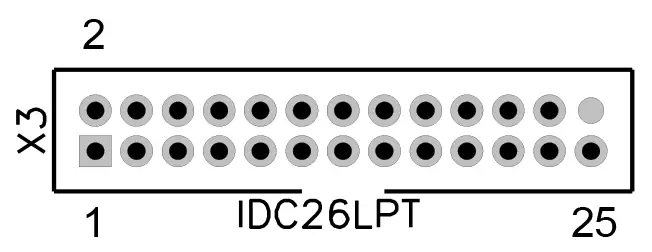
This connector is intended for a printer. An EPSON-compatible printer is recommended. Pin numbering starts at the square pad.
| № | Name | Description | № | Name | Description |
|---|---|---|---|---|---|
| 1 | STROBE | Strobe signal | 2 | Not used | |
| 3 | DATA0 | Data bit 0 | 4 | ERROR | Error signal |
| 5 | DATA1 | Data bit 1 | 6 | Not used | |
| 7 | DATA2 | Data bit 2 | 8 | Not used | |
| 9 | DATA3 | Data bit 3 | 10 | GND | Ground |
| 11 | DATA4 | Data bit 4 | 12 | GND | Ground |
| 13 | DATA5 | Data bit 5 | 14 | GND | Ground |
| 15 | DATA6 | Data bit 6 | 16 | GND | Ground |
| 17 | DATA7 | Data bit 7 | 18 | GND | Ground |
| 19 | Not used | 20 | GND | Ground | |
| 21 | BUSY | Busy signal | 22 | GND | Ground |
| 23 | PE | Paper-out signal | 24 | GND | Ground |
| 25 | Not used | 26 | KEY | Key (no pin) |
2.4. X4. JTAG for the EP1K50Q208 FPGA
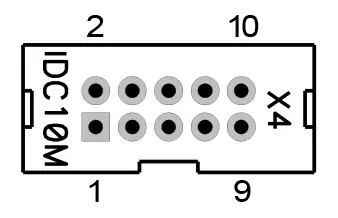
This connector programs the EP1K50Q208 FPGA through its JTAG interface using a ByteBlasterMV or another compatible programmer. Pin numbering starts at the square pad.
| № | Name | Description | № | Name | Description |
|---|---|---|---|---|---|
| 1 | TCK | Clock | 2 | GND | Ground |
| 3 | TDO | Data output | 4 | 3V3 | +3.3 V supply |
| 5 | TMS | Mode select | 6 | Not used | |
| 7 | Not used | 8 | Not used | ||
| 9 | TDI | Data input | 10 | GND | Ground |
2.5. X5. AVR ISP for the ATMEGA128 peripheral controller
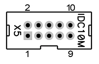
This connector programs the ATMEGA128 peripheral controller through its ISP interface using a ByteBlasterMV or another compatible programmer. Pin numbering starts at the square pad.
| № | Name | Description | № | Name | Description |
|---|---|---|---|---|---|
| 1 | CK | Clock | 2 | GND | Ground |
| 3 | DO | Data output | 4 | VCC5 | +5 V supply |
| 5 | RST | Reset | 6 | Not used | |
| 7 | Not used | 8 | EXCLOCK | External clock | |
| 9 | DI | Data input | 10 | GND | Ground |
2.6. X6. RS232 communication port
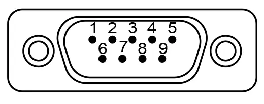
The communication port connects the board to another computer or to communication equipment, such as a modem.
| № | Name | Description | № | Name | Description |
|---|---|---|---|---|---|
| 1 | Not used | 6 | Not used (connected to pin 4) | ||
| 2 | RXD | 7 | RTS | ||
| 3 | TXD | 8 | CTS | ||
| 4 | Not used (connected to pin 6) | 9 | Not used | ||
| 5 | GND | Ground | Shell | Connector shell connected to ground | |
2.7. X7. VGA video output
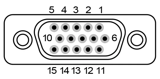
This connector accepts a monitor or television equipped with a VGA connector.
Warning: a VGA connector alone does not guarantee compatibility. For full compatibility, the monitor must support 50 Hz vertical and 31 kHz horizontal scan frequencies.
| № | Name | Description | № | Name | Description |
|---|---|---|---|---|---|
| 1 | R | Red video component | 9 | VIDEOVCC | Not used, or +5 V when jumper J3 is closed |
| 2 | G | Green video component | 10 | GND | Ground |
| 3 | B | Blue video component | 11 | GND | Ground |
| 4 | Not used | 12 | Not used | ||
| 5 | Not used | 13 | HS | Horizontal sync | |
| 6 | GND | Ground | 14 | VS | Vertical sync |
| 7 | GND | Ground | 15 | CSYNC | Not used, or composite sync when jumper J2 is closed |
| 8 | GND | Ground | Shell | Connector shell connected to ground | |
2.8. X8. RGB video output with composite sync
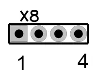
This connector provides RGB and composite sync for a television, monitor or PAL encoder. Use it together with X9 to connect a NedoPC PAL encoder.
Pin numbering starts at the square pad.
| № | Name | Description | № | Name | Description |
|---|---|---|---|---|---|
| 1 | R | Red video component | 2 | G | Green video component |
| 3 | B | Blue video component | 4 | CSYNC | Composite sync |
2.9. X9. Video output power
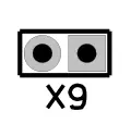
- GND — ground.
- VIDEOVCC — +5 V supply.
Use this connector together with X8 to connect a NedoPC PAL encoder.
Pin numbering starts at the square pad.
2.10. X10. 3.5 mm audio output
This connector accepts speakers, headphones and other audio playback or recording equipment.
The connector shell is connected to ground.
2.11. X11. PS/2 keyboard and mouse
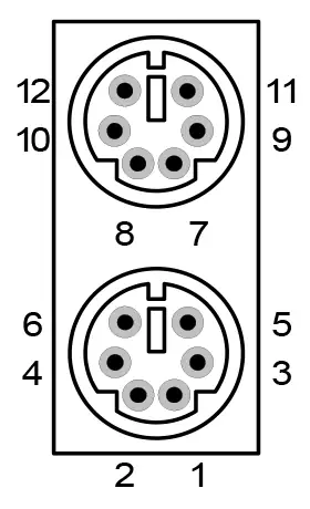
This connector accepts a PS/2 keyboard and mouse.
Connect the keyboard to the socket nearest the board and the mouse to the socket furthest from the board.
The connector shell is connected to ground.
| № | Name | Description | № | Name | Description |
|---|---|---|---|---|---|
| 1 | DATA | Keyboard data | 7 | DATA | Mouse data |
| 2 | Not used | 8 | Not used | ||
| 3 | GND | Ground | 9 | GND | Ground |
| 4 | +5V | +5 V supply | 10 | +5V | +5 V supply |
| 5 | CLK | Keyboard clock | 11 | CLK | Mouse clock |
| 6 | Not used | 12 | Not used |
2.12. X12. Original ZX keyboard and joystick
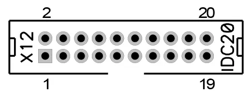
This connector accepts an original ZX keyboard and a Kempston joystick.
Pin numbering starts at the square pad.
| № | Name | Description | № | Name | Description |
|---|---|---|---|---|---|
| 1 | ZXROW0 | ZX keyboard row 0 | 2 | ZXROW1 | ZX keyboard row 1 |
| 3 | ZXROW2 | ZX keyboard row 2 | 4 | ZXROW3 | ZX keyboard row 3 |
| 5 | ZXROW4 | ZX keyboard row 4 | 6 | ZXROW5 | ZX keyboard row 5 |
| 7 | ZXROW6 | ZX keyboard row 6 | 8 | ZXROW7 | ZX keyboard row 7 |
| 9 | RST | Reset signal | 10 | ZXCOL4 | ZX keyboard column 4 |
| 11 | ZXCOL3 | ZX keyboard column 3 | 12 | ZXCOL2 | ZX keyboard column 2 |
| 13 | ZXCOL1 | ZX keyboard column 1 | 14 | ZXCOL0 | ZX keyboard column 0 |
| 15 | GND | Ground | 16 | JOYL | Joystick left |
| 17 | JOYR | Joystick right | 18 | JOYU | Joystick up |
| 19 | JOYD | Joystick down | 20 | JOYF | Joystick fire |
2.12.1. Connecting Kempston and Sinclair joysticks
| Sinclair 1 | Sinclair 2 | Kempston | |||||
|---|---|---|---|---|---|---|---|
| Function | ZX key | X12 pins to connect | Function | ZX key | X12 pins to connect | Function | X12 pins to connect |
| Left | 1 | 4–14 | Left | 6 | 5–10 | Left | 15–16 |
| Right | 2 | 4–13 | Right | 7 | 5–11 | Right | 15–17 |
| Down | 3 | 4–12 | Down | 8 | 5–12 | Up | 15–18 |
| Up | 4 | 4–11 | Up | 9 | 5–13 | Down | 15–19 |
| Fire | 5 | 4–10 | Fire | 0 | 5–14 | Fire | 15–20 |
2.13. X13. Mini USB (USB-to-RS232 bridge)
This connector links the board to a host computer in USB slave mode.
It provides a connection to computers that do not have an RS232 port.
2.14. X14. AVR JTAG for the ATMEGA128 peripheral controller
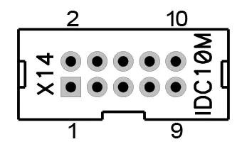
This connector programs the ATMEGA128 peripheral controller through the JTAG ICT interface using a compatible programmer.
Pin numbering starts at the square pad.
| № | Name | Description | № | Name | Description |
|---|---|---|---|---|---|
| 1 | TCK | Clock | 2 | GND | Ground |
| 3 | TDO | Data output | 4 | VCC | +5 V supply |
| 5 | TMS | Mode select | 6 | PRGRST | Reset |
| 7 | VCC | +5 V supply | 8 | Not used | |
| 9 | TDI | Data input | 10 | GND | Ground |
2.15. X15. Tape input and output
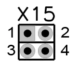
This connector provides input and output signals for tape-based data storage.
Pin numbering starts at the square pad.
| № | Name | Description | № | Name | Description |
|---|---|---|---|---|---|
| 1 | IN | Tape signal input | 2 | GND | Ground |
| 3 | OUT | Tape signal output | 4 | GND | Ground |
2.16. X16. Audio output (duplicates X10)
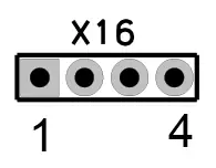
This audio output duplicates X10. It accepts speakers, headphones and other audio playback or recording equipment.
Pin numbering starts at the square pad.
| № | Name | Description | № | Name | Description |
|---|---|---|---|---|---|
| 1 | LOUT | Left channel output | 2 | GND | Ground |
| 3 | GND | Ground | 4 | ROUT | Right channel output |
2.17. X17, X18 and X20. Audio inputs
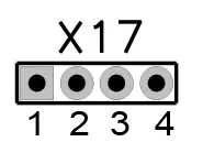
These audio inputs accept external sound sources, such as a CD-ROM drive or NeoGS.
Pin numbering starts at the square pad.
| № | Name | Description | № | Name | Description |
|---|---|---|---|---|---|
| 1 | LIN | Left channel input | 2 | GND | Ground |
| 3 | GND | Ground | 4 | RIN | Right channel input |
2.18. X19. RS232 communication port (duplicates X6)
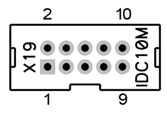
The communication port connects the board to another computer or to communication equipment, such as a modem.
Pin numbering starts at the square pad.
| № | Name | Description | № | Name | Description |
|---|---|---|---|---|---|
| 1 | Not used | 2 | RXD | ||
| 3 | TXD | 4 | Not used (connected to pin 6) | ||
| 5 | GND | Ground | 6 | Not used (connected to pin 4) | |
| 7 | RTS | 8 | CTS | ||
| 9 | Not used | 10 | +5V | +5 V supply |
2.19. X21. Tape IN (duplicates the input on X15)
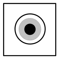
An input for loading software from a tape recorder or a similar signal source.
2.20. PWR1. Power connector
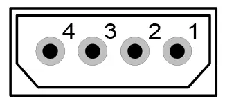
A connector for a non-standard power supply.
| № | Name | Description | № | Name | Description |
|---|---|---|---|---|---|
| 1 | VCC5 | +5 V supply | 3 | GND | Ground |
| 2 | GND | Ground | 4 | VCC12 | +12 V supply |
2.21. PWR2. ATX power connector
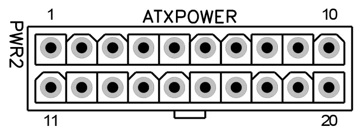
This connector powers the ZX Evolution board from a standard ATX power supply.
| № | Name | Description | № | Name | Description |
|---|---|---|---|---|---|
| 1 | Not used | 11 | Not used | ||
| 2 | Not used | 12 | Not used | ||
| 3 | GND | Ground | 13 | GND | Ground |
| 4 | VCC5 | +5 V supply | 14 | PS_ON | Power on |
| 5 | GND | Ground | 15 | GND | Ground |
| 6 | VCC5 | +5 V supply | 16 | GND | Ground |
| 7 | GND | Ground | 17 | GND | Ground |
| 8 | PWRGOOD | Power good | 18 | Not used | |
| 9 | VCC5STBY | +5 V standby supply | 19 | VCC5 | +5 V supply |
| 10 | VCC12 | +12 V supply | 20 | VCC5 | +5 V supply |
2.22. GB1. Clock battery holder
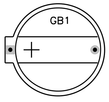
This holder accepts a battery to power the non-volatile memory and the PCF8583 clock.
A 3 V CR2032 battery is recommended.
3. Jumpers and buttons
| № | Name | Default | Description |
|---|---|---|---|
| J1 | enable IDERES | Open | When closed, routes RESET to the IDE connector so that IDE devices can be reset through the interface. Required by some older hard drives, including certain Samsung models. |
| J2 | enable composite sync to VGA | Open | When closed, routes composite sync to the VGA connector. |
| J3 | enable +5V to VGA | Open | When closed, supplies +5 V to the VGA connector. |
| J4 | 12v enable | Open | When closed, supplies +12 V to the expansion slots. |
| J5 | external clock | Open | When closed, allows the ATMEGA128 to use an external clock connected through the AVR ISP connector (X5). |
| J6 | soft reset key | Open | This pair of contacts serves two purposes:
|
| J7 | HRDY->IP | Open | When closed, HRDY pulls the IP signal to GND. |
| J8 | NMI key | Open | When closed, asserts NMI on the Z80 processor. |
| J9 | hard reset key | Open | When closed, resets the computer, including the ATMEGA128. Intended for the Reset button of an AT or ATX case. |
| VD32 | HDD Led | Connection for the HDD LED of an AT or ATX case. | |
| VD63 | PWR Led | Connection for the PWR LED of an AT or ATX case. |
2 If a pair of header pins is fitted instead of LED VD3, as on assembled boards supplied by NedoPC.
3 If a pair of header pins is fitted instead of LED VD6, as on assembled boards supplied by NedoPC.
4. ZXBUS slots
ZX Evolution has two ZXBUS-compatible expansion slots.
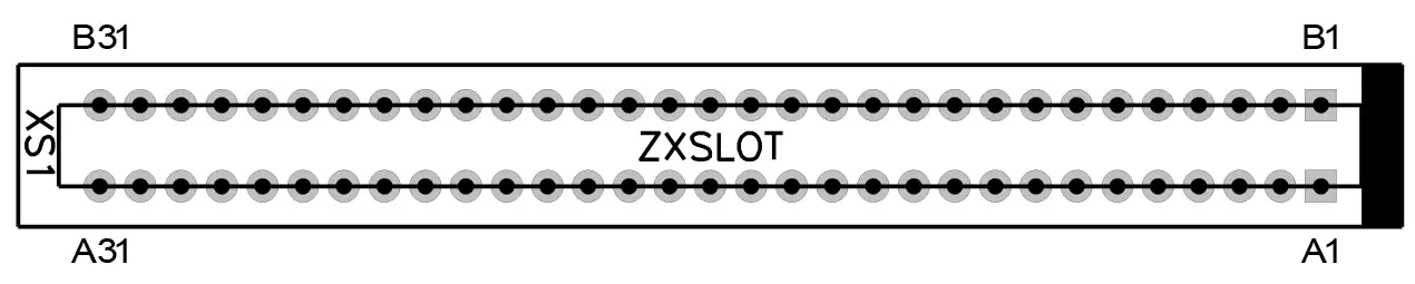
The ZXBUS contact pitch is 2.54 mm. Take care when fitting expansion cards made in the 1990s or earlier: they may use a 2.5 mm pitch.
The first contact in each row is marked by a square pad. When the board is installed in an ATX case, pin 1 is nearest the rear of the case.
Warning: when fitting an expansion card, make sure its locating tab is at the pin 1 end of the slot. If the card has no locating tab, check the documentation supplied with it. Incorrect installation can destroy components on both the expansion card and the computer.
Warning: the ZX Evolution manufacturer accepts no responsibility for incompatibility or damage caused by third-party expansion cards and does not undertake to test such cards. Contact the expansion-card manufacturer about compatibility.
Note: if an expansion card requires +12 V, fit a jumper across J4.
| № | Name | Description | № | Name | Description |
|---|---|---|---|---|---|
| A1 | A14 | Processor address bus bit 14 | B1 | A15 | Processor address bus bit 15 |
| A2 | A12 | Processor address bus bit 12 | B2 | A13 | Processor address bus bit 13 |
| A3 | +5V | +5 V supply | B3 | D7 | Processor data bus bit 7 |
| A4 | DCDOS | TRDOS ROM window active | B4 | Not used | |
| A5 | Not used | B5 | Not used | ||
| A6 | GND | Ground | B6 | D0 | Processor data bus bit 0 |
| A7 | GND | Ground | B7 | D1 | Processor data bus bit 1 |
| A8 | Not used | B8 | D2 | Processor data bus bit 2 | |
| A9 | A0 | Processor address bus bit 0 | B9 | D6 | Processor data bus bit 6 |
| A10 | A1 | Processor address bus bit 1 | B10 | D5 | Processor data bus bit 5 |
| A11 | A2 | Processor address bus bit 2 | B11 | D3 | Processor data bus bit 3 |
| A12 | A3 | Processor address bus bit 3 | B12 | D4 | Processor data bus bit 4 |
| A13 | IORQGE | Inhibit signal for other devices | B13 | INT | Interrupt |
| A14 | GND | Ground | B14 | NMI | Non-maskable interrupt |
| A15 | CSROMCE | ROM chip enable | B15 | HALT | Processor halt |
| A16 | RS | ROM window switching signal | B16 | MREQ | Processor memory request |
| A17 | Not used | B17 | IORQ | Processor I/O request | |
| A18 | Not used | B18 | RD | Processor read | |
| A19 | BUSRQ | DMA request | B19 | WR | Processor write |
| A20 | RES | Reset signal | B20 | Not used | |
| A21 | A7 | Processor address bus bit 7 | B21 | WAIT | Wait |
| A22 | A6 | Processor address bus bit 6 | B22 | Not used | |
| A23 | A5 | Processor address bus bit 5 | B23 | Not used | |
| A24 | A4 | Processor address bus bit 4 | B24 | M1 | Start of an instruction cycle |
| A25 | CSROM | ROM selected | B25 | RFSH | Memory refresh |
| A26 | BUSAK | DMA acknowledge | B26 | A8 | Processor address bus bit 8 |
| A27 | A9 | Processor address bus bit 9 | B27 | A10 | Processor address bus bit 10 |
| A28 | A11 | Processor address bus bit 11 | B28 | +5V | +5 V supply |
| A29 | +5V | +5 V supply | B29 | +12V | +12 V supply |
| A30 | GND | Ground | B30 | GND | Ground |
| A31 | XS1: IORQGE2; not used on XS2 | B31 | XS1: IORQ2; not used on XS2 |
5. ZX Evolution firmware
ZX Evolution contains an ATMEGA128 microcontroller and a 29F040 ROM chip.
The ATMEGA128 microcontroller performs three functions:
- It manages external peripherals and translates their signals into the interfaces expected by the ZX Spectrum.
- It loads firmware into the EP1K50QC208 FPGA at power-on or after a hardware reset.
- It allows the computer configuration to be updated by replacing the writable part of the microcontroller firmware.
The ATMEGA128 firmware consists of two parts:
BOOTLOADER
BOOTLOADER is the fixed part of the firmware used to replace or update the writable part of the microcontroller firmware. Refer to the bootloader documentation for details.
It can only be written with a hardware programmer on the assembled board. The microcontroller supplied in a self-assembly kit does not contain firmware.
Updating the bootloader also requires a hardware programmer. The website provides bootloader binaries for two types of programmer.
Configuration
The configuration is the writable part of the firmware. It manages peripherals and loads the computer configuration.
Configurations may be supplied by different developers. Special service configurations are also available for setting up and testing a newly assembled computer.
Configurations are distributed as specially prepared zxevo_fw.bin files.
Note: NedoPC develops and maintains two configurations:
- TEST&SERVICE — for setting up and testing the computer after assembly and for programming or updating the 29F040 ROM chip.
- BASECONF — the reference configuration, developed by NedoPC according to its vision for the evolution of the ZX Spectrum. Third-party developers may use its source code as a starting point for their own configurations.
Warning: NedoPC does not maintain or support third-party configurations and accepts no responsibility for incorrect operation of ZX Evolution when they are used.
29F040 ROM image
The 29F040 ROM firmware contains the routines needed to operate the computer in ZX Spectrum mode, including Basic48, Basic128 and TRDOS.
It is distributed as zxevo.rom, a binary file containing the complete image to be written to the 29F040 ROM. Third-party developers may assemble their own ROM contents.
Updating and restoring the ROM
Use the TEST&SERVICE configuration to update or restore the ROM image:
- Load TEST&SERVICE using BOOTLOADER.
- Copy zxevo.rom to an SD card and insert the card into the computer.
- Select the appropriate item in the TEST&SERVICE menu and program the ROM.
- Use BOOTLOADER to load the working configuration, such as BASECONF.
Note: NedoPC supplies its own ROM image based on EVO RESET SERVICE. This image is designed to work with NedoPC’s BASECONF configuration.
Update the working configuration and ROM image together. Combining an old ROM image with a new configuration, or vice versa, may cause malfunctions.
EVO RESET SERVICE can update the ROM image from within its own interface. See its documentation for details.
6. Installing the board in an ATX, microATX or mini-ITX case
The ZX Evolution board is designed for straightforward installation in a standard ATX, microATX or mini-ITX case.
Note: mounting hardware and blanking plates are not included with the ZX Evolution board.
Installation steps
- Insert a CR2032 or equivalent battery into holder GB1 on the board.
- Place the board on the mounting points of the case tray and secure it with screws. Install the tray in the case. Connectors X21, X10, X7, X13, X6, XSD1 and X11 should face the rear I/O opening.
- Connect the power supply cable to PWR2.
- Connect the case Reset button cable, RES SW, to the J9 hard reset contacts.
- Connect the case Power button cable, PWR SW, to the J6 soft reset contacts.
- Connect the case drive-activity LED cable, IDE LED, to VD34. The positive contact has a square pad.
- Connect the case Power LED cable, PWR LED, to VD65. The positive contact has a square pad.
- Install the floppy drive or drives6, connect their power cables and connect their ribbon cable to X1.
Warning: the floppy cable differs from a standard PC cable. See the example in the floppy-drive appendix. - Install the IDE device or devices7, connect their power cables and connect their ribbon cable to X2.
Warning: two IDE devices must be configured as master and slave.
Power control
Power control differs slightly from that of a conventional PC:
| Operation | Action |
|---|---|
| Power on (ATX power supply) |
|
| Power off (ATX power supply) |
|
| Processor reset |
|
| Hard reset |
|
4 If a pair of header pins is fitted instead of LED VD3, as on assembled boards supplied by NedoPC.
5 If a pair of header pins is fitted instead of LED VD6, as on assembled boards supplied by NedoPC.
6 A floppy drive is optional; the board can operate without one.
7 An IDE device is optional; the board can operate without one.
7. Appendix 1. Connecting a display
ZX Evolution supports two types of display:
- VGA monitors;
- televisions.
Connect a VGA monitor to X7. Enable the corresponding display mode on ZX Evolution.
Note: VGA/TV mode is switched from the keyboard. With NedoPC BASECONF firmware, use Scroll Lock. The keyboard Scroll Lock LED is lit in VGA mode.
Warning: make sure a VGA monitor supports a 48.8 Hz refresh rate. A list of tested monitors is available on the ZX Evolution project website8.
ZX Evolution revision C provides a dedicated connection for an RGB monitor, for example through SCART-RGB, or a PAL encoder. It consists of two headers: X8 and X9.
Connecting a PAL encoder
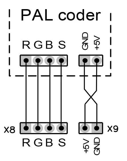
Make an adapter cable for the PAL encoder as shown in the diagram.
Connecting a television through SCART
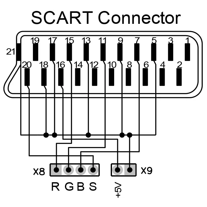
Make a SCART adapter cable for the television as shown in the diagram.
Warning: the television must support RGB input through SCART.
A television or PAL encoder can also be connected to the appropriate pins of the VGA connector X7, following the diagrams above. Close J2 and J3 to make composite sync and power available on X7.
8. Appendix 2. Connecting floppy drives
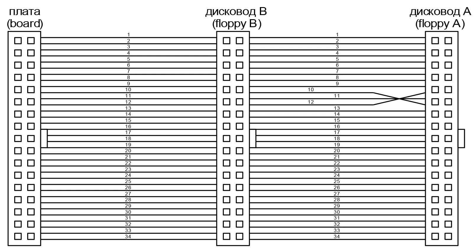
A PC floppy controller selects drives differently and supports only two drives on a ribbon cable. The ZX Evolution controller, based on the KR1818VG93 (WDC1793), can work with up to four drives.
Connecting a 5.25-inch drive
Set a 5.25-inch floppy drive to DD (720 KB) mode and drive number 0 or A, usually with the DS (drive select) jumper. Check the drive documentation for the correct settings.
Connecting two 3.5-inch drives
The drive-select jumper on a PC 3.5-inch floppy drive is normally fitted or soldered so that ZX Evolution identifies it as drive B, the second drive. To connect two PC 3.5-inch drives without modifying them, make the special ribbon cable shown below:
Using DD and HD disks
TRDOS uses DD disks and DD drive mode. Some later 3.5-inch drives do not support DD mode. In that case, modify the drive or use a model that supports DD operation.
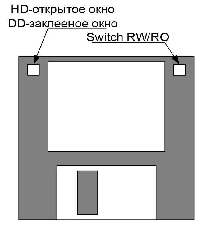
To use a 3.5-inch HD disk, cover its density-detection hole so that the drive detects it as a DD disk.
9. Appendix 3. Additional PS/2 keyboard functions
These functions apply only to the baseconf configuration with the EVO reset service ROM.
| PS/2 keyboard shortcut | Function |
|---|---|
| F12 | Soft reset. Equivalent to the soft reset contacts (J6) on the board. Resets only the Z80 processor, without reloading the computer configuration. Warning: holding F12 for 5 seconds switches off the power when using an ATX power supply. |
| Ctrl + Alt + Del | Hard reset. Equivalent to the hard reset contacts (J9) on the board. Resets the ZXEvo board and reloads its configuration. |
| ScrollLock | Switches the video output between VGA and TV modes. The keyboard ScrollLock LED is lit in VGA mode. |
| PrintScreen | Generates an NMI (non-maskable interrupt) on the Z80 processor. |
| NumLock | Switches the audio output between tapeout (tape output) and beeper (sound output) modes. The keyboard NumLock LED is lit in tapeout mode. |
| Left mouse button + right mouse button + * on the numeric keypad | Restores the default mouse resolution. |
| Left mouse button + right mouse button + + on the numeric keypad | Increases the mouse resolution. |
| Left mouse button + right mouse button + − on the numeric keypad | Decreases the mouse resolution. |
| 0 (zero) + F12 | Press 0, keep it held down and press F12. Release F12, then release 0. Sets the main firmware mode to Evo service. |